In a typical buck converter shown in Fig. 1, the output ripple voltage is an important design specification. Sensitive loads may specify a maximum ripple voltage. The max allowable voltage for the load is also limited by the ripple, especially for loads with tight specifications such as many processors.
The output ripple voltage is given by
\[ \Delta V_\mathrm{out} = \frac{V_\mathrm{in}D(1-D)}{8LCf_\mathrm{sw}^2} \]
The derivation is given at the end of this post for those interested. The different parameters are:
- \( \Delta V_\mathrm{out} \) = peak-to-peak output ripple voltage
- \( V_\mathrm{in} \) = input voltage
- \( D \) = duty cycle
- \( L \) = inductance
- \( C \) = output capacitance
- \( f_\mathrm{sw} \) = switching frequency
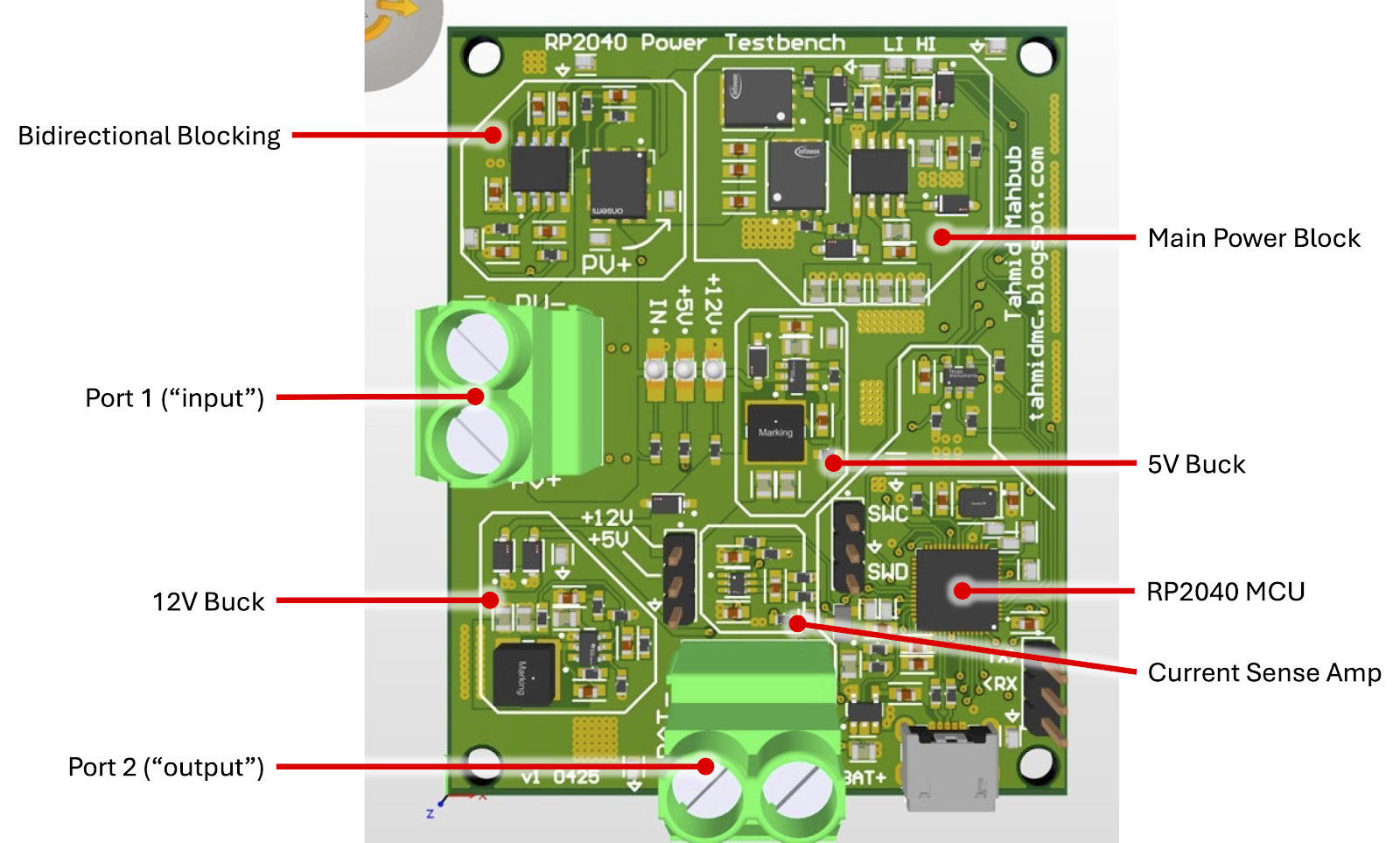
We can look at the output ripple using the power testbench. The converter is run at 50kHz and 50% duty cycle, with varying input voltages. The output capacitor of the converter is the parallel combination of 4x 0805 10µF caps (GRM21BR61H106KE43) and 1x 1206 10µF cap (CGA5L3X5R1H106K160AB). The inductor is rated at 5.6µH, specifically the Wurth 732-3799-1-ND.
Based on this, you would expect the output ripple at 10V input to be given by:
\[ \Delta V_\mathrm{out} = \frac{V_\mathrm{in}D(1-D)}{8LCf_\mathrm{sw}^2} = \frac{10V \cdot 0.5 \cdot 0.5}{8\cdot 5.6\mu H \cdot 50\mu F \cdot (50\;kHz)^2} =0.45\;V \]
The ripple waveform is obtained with a scope that is AC coupled and can be seen below in Fig. 2. From the scope shot, it appears that the voltage ripple is about 0.75V, which is a fair bit higher than the expected ripple. So what gives?
Fig. 2 - Output ripple, AC coupled, 500mV/division, Vin=10V, Vout=5V
The culprit here is voltage derating of ceramic capacitors. Much like how I've previously written about
electrolytic capacitors derating with frequency, ceramic capacitors (particularly class II dielectrics) can derate substantially with voltage. This has to do with the reduced permittivity of the dielectric, reducing the capacitors' ability to store energy at higher voltage biases. This is often given in manufacturer technical documentation. For our caps, the derating charts are reproduced below.
Fig. 4b -
CGA5L3X5R1H106K160AB 5V DC bias corresponds to a 9.1µF capacitance; you will often notice that larger packages correspond to reduced derating and hence have larger capacitances for the same initial capacitance and voltage rating
Considering the derating from Figs. 3-4, the total output capacitance is 34µF. With this new value plugged in, the expected output ripple is about
\[ \Delta V_\mathrm{out} = \frac{V_\mathrm{in}D(1-D)}{8LCf_\mathrm{sw}^2} = \frac{10V \cdot 0.5 \cdot 0.5}{8\cdot 5.6\mu H \cdot 34.7\mu F \cdot (50\;kHz)^2} =0.64\;V \]
This is much closer to the observed value with a 14.5% error, something that is fairly within the tolerance of different components.
If we now look at the results with 20V input (corresponding to 10V output), we would expect an output ripple of double that for the 10V input, corresponding to 1.3V; if the caps didn't further derate. However, we can find again from the manufacturer data that the total output capacitance is 19.7µF, down from 34µF, which would correspond to a greater increase in the ripple. This is shown in Figs. 5a and 5b.
Fig. 6 - Output ripple, AC coupled, 500mV/division, Vin=20V, Vout=10V
The output ripple observed with 20V input is shown in Fig. 6. The measured ripple corresponds to 2.7V, which further highlights the substantial capacitance drop with 10V bias for the output ceramic capacitors!
The expected ripple with ideal caps is given by
\[ \Delta V_\mathrm{out} = \frac{V_\mathrm{in}D(1-D)}{8LCf_\mathrm{sw}^2} = \frac{20V \cdot 0.5 \cdot 0.5}{8\cdot 5.6\mu H \cdot 50\mu F \cdot (50\;kHz)^2} = 0.9\;V \]
However, with derated capacitance, the expected ripple is
\[ \Delta V_\mathrm{out} = \frac{V_\mathrm{in}D(1-D)}{8LCf_\mathrm{sw}^2} = \frac{20V \cdot 0.5 \cdot 0.5}{8\cdot 5.6\mu H \cdot 19.7\mu F \cdot (50\;kHz)^2} = 2.3\;V \]
This is much closer to the observed ripple value.
For proper filtering, it is crucial to consider the DC bias impact on the ceramic capacitors and the corresponding derating, in addition to component tolerance! Otherwise, the filtering will be insufficient and the ripple will be much higher than expected, as shown here. This could result in poor circuit performance or even component damage!
Note that the circuit parameters here were chosen to have large output ripple to illustrate the concern described in this article. In almost any application, this circuit has a very high ripple percentage. Even with the components as present, the frequency can be increased substantially to reduce the ripple. Alternately, the output inductor or capacitance can be increased.
Ripple Derivation
Fig. D1 - Buck Converter
Fig. D2 - Buck Converter when QH is on
Fig. D3 - Buck Converter when QL is on
To find the output ripple in a buck converter, we start from the inductor current, which can be determined from the inductor voltage in either QH on or QL on state. We can identify that \( i_\mathrm{L} \) increases when QH is on since \( v_\mathrm{L} \) is positive then. And similarly, \( i_\mathrm{L} \) decreases when QL is on since \( v_\mathrm{L} \) is negative.
QH is on for a fraction of the switching period given by the duty cycle D. For a buck converter, the output voltage is given by \( V_\mathrm{out} = D V_\mathrm{in} \). The inductor voltage relationship \( v_\mathrm{L} = L \frac{di_\mathrm{L}}{dt} \) can be rewritten for constant voltage \( v_\mathrm{L} = L \frac{\Delta i_\mathrm{L}}{\Delta t} = L \frac{\Delta i_\mathrm{L}}{D T_\mathrm{sw}} \) where \(T_\mathrm{sw}\) is the switching period.
The peak-to-peak inductor current ripple is thus given by
\[ \Delta i_\mathrm{L,pp} = \frac{V_\mathrm{in}-V_\mathrm{out}}{L}\cdot \frac{D}{f_\mathrm{sw}} = \frac{V_\mathrm{in}(1-D)D}{Lf_\mathrm{sw}} \]
We know from Fig. D1 that \( i_\mathrm{L} = i_\mathrm{C} + i_\mathrm{out} \). We can find the impedance of the output capacitor and determine the current split between it and the output load. We can assume (and confirm mathematically) that the impedance of the output cap at high frequencies (such as in a typical buck converter) is much lower than the load resistance. Thus, we can assume that the inductor ripple current is going through the output cap, as shown in Fig. D4, and that the DC amount is going through the load resistor.
Fig. D4 - Current going through the output capacitor
When the ripple current is positive (for half of \( T_\mathrm{sw} \) ), the output capacitor is charged and when the ripple current is negative, the output capacitor is discharged. The peak-to-peak capacitor voltage ripple can be found from the positive inductor current charging the cap, where Q is the charge \( \int i_\mathrm{C}\;dt = \frac{1}{2} \frac{\Delta i_\mathrm{L,pp}}{2} \frac{T_\mathrm{sw}}{2} = \frac{1}{8} \Delta \frac{i_\mathrm{L,pp}}{f_\mathrm{sw}} \)
\[ \Delta V_\mathrm{out} = \frac{Q}{C} = \frac{1}{8Cf_\mathrm{sw}} \Delta {i_\mathrm{L,pp}} = \frac{1}{8Cf_\mathrm{sw}} \frac{V_\mathrm{in}(1-D)D}{Lf_\mathrm{sw}} = \boxed{ \frac{V_\mathrm{in}D(1-D)}{8LCf_\mathrm{sw}^2} } \]
As a final check, we can go back to checking the magnitude of the output capacitance compared to the load resistance (10Ω output resistor was used) with the circuit in Fig. 0.
\[ |Z_\mathrm{C}| = \frac{1}{2 \pi f_\mathrm{sw} C} = \frac{1}{2 \pi 50\;kHz \; 19.7\mu F} = 0.16 \Omega \ll 10 \Omega \]