Principle of Phase Angle Control
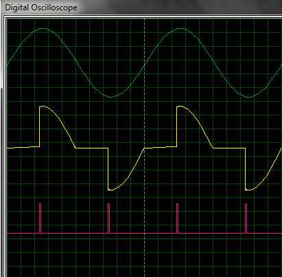
Top - Output Voltage
Bottom - Gate Drive Signal
Image source: Wikipedia (http://en.wikipedia.org/wiki/File:Regulated_rectifier.gif)
The
photo above clearly illustrates phase angle control: output voltage
controlled by the gate drive signal applied to a thyristor. What is
phase angle control? That is what I'm going to talk about in this
article.
Phase angle control is a method of PWM applied to AC input
voltages, usually the mains supply. Of course, the AC supply could be from a
transformer or any other AC source, but the mains supply is the most common
input – this gives the phase angle control method its greatest usefulness. It
has of course become quite obvious from the title (and I’m sure most of you
reading will already know this) that the purpose of phase angle control is to
control or limit power to the load.
The power device used in phase angle controllers is a
thyristor – mostly triacs or SCRs. (There are methods of phase controlling
employing high frequency switching using a MOSFET or IGBT, but here I’ll talk
about phase angle control with thyristors only). The power flow to the load is
controlled by delaying the firing angle (firing time each half-cycle) to the
power device.
We know that the thyristor is a latching device – when the
thyristor is turned on by a gating signal and the current is higher than the
holding current and the latching current, the thyristor stays on, until the
current through it becomes sufficiently low (very close to zero). The thyristor
turns off when current through it becomes zero, as happens at the AC mains zero
crossing. This is the natural line commutation. (Another method of turning the
thyristor off is by forced commutation. I won’t go into that now.) The
assumption here is that the load is resistive and has little to no inductance.
Of course, this is not always the case, as inductive loads are often used.
However, I’ll work with this assumption for now.
Now, with that covered, you should read this article first
before proceeding to the rest of this article:
I’ve added the circuit, code and simulation of an example
later in this article. And that uses a triac as the power device. So, from now
on, I’ll just refer to the triac instead of talking about a thyristor in
general.
So, in phase angle control, a gate pulse is sent to the
triac. This is sent at a time between one zero crossing and the next. Without
the gate pulse sent to the triac, right after zero-crossing, the triac is off
and no current flows through it. After a certain time, the gating signal is
given to the triac and it turns on. The triac then stays on until the current
through it becomes zero (natural line commutation). This is at the next zero
crossing. For simplicity’s sake and as usually should be, assume that the
current through the triac (when on) is larger than the latching current and the
holding current. If you didn’t already know this, the latching current is the
current that must pass through the triac right after it is turned on to ensure
that it latches. The holding current is the current level through the triac
below which the triac will turn off. So, the assumption that current through
the triac is higher than the latching current and the holding current means
that the triac stays on once it is fired on. It stays on until the current
through it is zero.
This means that the voltage is supplied to the load for a
fraction of the cycle, determined by how long the triac is on. How long the
triac is on, is, in turn, determined by the delay time between the
zero-crossing and the applying of the triac gating signal.
So, to sum it up, we adjust the voltage or power delivered to
the load by delaying the trigger signal to the triac. One thing to remember is
that, the delivered voltage and power are not linearly related to the firing
phase angle.
There are two voltages here that we are concerned with – the
RMS voltage and the average voltage. The RMS voltage governs the power output
to resistive loads such as incandescent bulbs and resistive heaters. The
average value relates to devices that function on the average voltage level. This
is important because, when testing, your voltmeter will register the average
voltage – and not the true RMS voltage – unless you have a “true RMS
voltmeter”. Most inexpensive voltmeters are not true RMS meters but will
respond to average value changes.
To clarify why power and voltage are not linearly related,
let’s examine the formula relating the two.
So, assuming a constant resistance (be
careful if you’re using incandescent lamps, since they are NOT constant
resistance devices), power is directly proportional to the square of the
voltage. So, if you half the voltage, the power is not halved, but is reduced to
one-fourth the original power! One-fourth power with half the voltage!
Now let’s now go on to the design part – how we’re actually
going to do this.
For
the microcontroller, I’ve chosen the extremely popular ATmega8. However,
since this application requires only a few pins, you can easily use any other
small microcontroller for this purpose, such as ATtiny13.
The
zero-crossing is done using the bridge-optocoupler method as I had previously
shown. For details regarding the zero-crossing, please go through the article:
Now, let’s take a look at the code:
//---------------------------------------------------------------------------------------------------------
//Programmer: Syed Tahmid Mahbub
//Compiler: mikroC PRO for AVR v2.10
//Target AVR: ATmega8
//Program for phase angle control - adjustable phase angle
//---------------------------------------------------------------------------------------------------------
unsigned char FlagReg;
unsigned char Count;
unsigned char i;
sbit ZC at FlagReg.B0;
void interrupt() org IVT_ADDR_INT0{
ZC = 1;
}
void main() {
DDRD = 0xFB; //PORTD all output except PD2 - INT0
PORTD = 4; //Clear PORTD and enable pullup on PD2
DDRB = 0; //PORTB all input
PORTB = 0xFF; //Enable pullups on PORTB
ISC01_bit = 1; //External interrupt on falling edge
ISC00_bit = 0;
INT0_bit = 1; //Enable ext int 0
INT1_bit = 0; //Disable ext int 1
SREG_I_bit = 1; //Enable interrupts
while (1){
if (ZC){ //zero crossing occurred
Count = (~PINB)+1;
for (i = 0; i < Count; i++){
delay_us(800);
}
PORTD.B0 = 1; //Send a pulse
delay_us(250);
PORTD.B0 = 0;
ZC = 0;
}
}
}
Take a look at the circuit diagram below. PORTB is connected to a DIP-switch.
Let me first talk about the DIP-switch. The DIP-switch I chose has 3
individual switches, each of which can take on or off position. So, the
DIP-switch can have 8 possible states and we can assign a digital value
to the DIP-switch states. Let's assume that switch 0 is the switch connected to PORTB0/PINB0,
that switch 1 is the switch connected to PORTB1/PINB1, and that switch 2 is the switch connected to PORTB2/PINB2. So,
the possible DIP-switch states with their assigned values are:
0 - switch 0, switch 1 and switch 2 are all off
1 - switch 0 on, switch 1 and switch 2 are off
2 - switch 0 off, switch 1 on and switch 2 off
3 - switch 0 and switch 1 on and switch 2 off
4 - switch 0 off, switch 1 off and switch 2 on
5 - switch 0 on, switch 1 off and switch 2 on
6 - switch 0 off, switch 1 and switch 2 on
7 - switch 0, switch 1 and switch 2 are all on
So, the DIP-switch can alter the values of PORTB0, PORTB1 and PORTB2. I made all of PORTB input pins and enabled the pull-ups. So, by default, all PORTB pins are high. When one of the switches is ON or shorted, that corresponding pin is low. So, only PORTB0, PORTB1 and PORTB2 can be switched to be high or low. The other pins will be high at all times. So, in order to read the value of the DIP-switch, I first inverted each individual bit of PORTB when reading (PINB) and then added 1 to the value as I wanted one to be the minimum value. Why one the minimum value? If you see the code later, you will see that the register "Count" is used to determine the delay time before the triac is fired. Count will have the value of the DIP-switch state plus one. I wanted a minimum delay before the triac is fired so that there is always a delay after the zero-crossing after the triac is fired. So, the function of the DIP-switch is now quite obvious. The DIP-switch sets the time after the zero-crossing after which the triac is fired. When only PORTB0/PINB0 is low, the delay time before firing the triac is minimum; it is equal to 800
µs. When PORTB0/PINB0, PORTB1/PINB1 and PORTB2/PINB2 are all low, the delay time before firing the triac is maximum; it is equal to 800
µs * 8 = 6.4ms. The adjusting delay time before firing adjusts the firing angle. How the time is related to the firing angle can be seen at the bottom of this article. The formula and an example are provided.
So, the program is basically as follows:
The zero-crossing is first checked.
After zero-crossing occurs, a small delay is present before the triac is fired. This delay is set by the value of the DIP-switch. So, the triac is fired a while after the zero-crossing occurs.
The gating signal is removed 250µs after that. 250µs
is enough time to ensure that the triac has turned on. Even though the
gating
signal is removed, the triac stays on until the next zero-crossing as it
is a
latching device. Now you may ask, why remove the gating signal? Just
keep it on till the next zero-crossing. Well, that'd work too. The
problem there would be that, there would be high switching losses of the
thyristor. The gate drive resistance would dissipate immense amounts of
power - all for no reason, since the triac would be on even if the
signal was removed.
In my circuit, I used the internal 4MHz RC oscillator. So, make sure you set the fuse bits correctly if you're using the internal oscillator.
The rest of the code should be easy to understand and should
be self-explanatory – I’ve added comments to help you understand.
Now let’s take a look at my circuit setup and then the different output waveforms using
this code:
Fig. 1 - Circuit Diagram (Click on image to enlarge)
You should choose R1 depending on the gate current
requirements of the triac. It must also have a sufficiently high power
dissipation rating. Usually, the instantaneous power may be very high. But
since current flows through the resistor for only 250us (1/40 of a 50Hz half cycle),
the average power is small enough. Usually, 2W resistors should suffice.
Let’s assume we’re using a BT139-600 triac. The maximum required trigger
current is 35mA. Although the typical trigger current is lower, we should
consider the maximum required trigger current. This is 35mA for quadrants I, II
and III. We will only be firing in quadrants I and III. So, that is ok for us –
we need to consider 35mA current.
If you aren’t sure what quadrants are, here’s a short
description. First take a look at this diagram:
Fig. 2 - Triac Triggering Quadrants
If you look back again at the diagram, you’ll see that we’re
driving gate from MT2. So, we can say that, with respect to MT1, when MT2 is
positive, so is the gate. With respect to MT1, when MT2 is negative, so is the
gate. From the diagram above, you can see that these two cases are in quadrants
I and III. This is what I meant when I mentioned that we’re driving only in
quadrants I and III.
The driver in the circuit is the MOC3021. This is a random
phase optically isolated triac output driver. When the LED is turned on, the
triac in the MOC3021 turns on and drives the main triac in the circuit. It is a
“random phase” driver meaning that it can be driven on at any time during the
drive signal, as is required for phase angle control. There are other drivers
that only allow drive at the zero-crossing. These cannot be used for phase
angle control as phase angle control requires drive after zero-crossing. For
guaranteeing that the triac is latched, the LED side of the MOC3021 must be
driven with at least 15mA current. The maximum current rating for the LED is
60mA. The peak current rating for the triac is 1A. You should find that we have
stayed within these limits in the design.
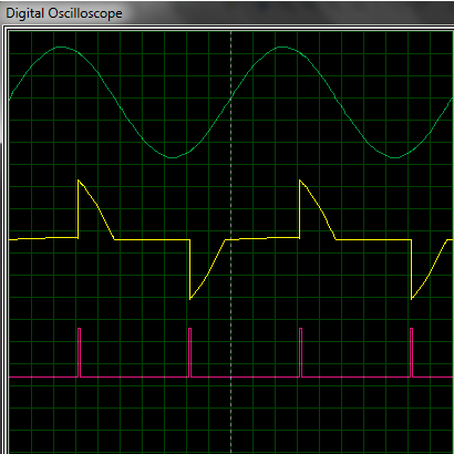
Here’s the output waveform with 800µs delay (all PORTB/PINB pins high : DIP-switch state = 0):
Fig. 3 - Triac firing with 800µs delay
Green: Input AC
Yellow: AC Output after phase angle control
Pink: Gate Drive signal
You can clearly see that before the gate driving signal is
applied, there is no output (illustrated by the flat yellow line).When the gate
driving signal is applied, the triac turns on. There is an output and the triac
stays on till the next zero crossing. After this again, there is no output till
the next gate drive signal is applied.
Now I’ll show you a few more waveforms, with other initial
delays.
Here, the gate is driven 1.6ms after the zero-crossing (only PORTB0/PINB0 low : DIP-switch state = 1):
Fig. 4 - Triac firing with 1.6 ms delay
Green: Input AC
Yellow: AC Output after phase angle control
Pink: Gate Drive signal
Here, the gate is
driven 2.4ms after the zero-crossing (only PORTB1/PINB1 low : DIP-switch state = 2):
Fig. 5 - Triac firing with 2.4 ms delay
Green: Input AC
Yellow: AC Output after phase angle control
Pink: Gate Drive signal
Here, the gate is driven 3.2ms after the zero-crossing (PORTB0/PINB0 and PORTB1/PINB1 low : DIP-switch state = 3):
Fig. 6 - Triac firing with 3.2 ms delay
Green: Input AC
Yellow: AC Output after phase angle control
Pink: Gate Drive signal
Here, the gate is driven 4ms after the zero-crossing (only PORTB2/PINB2 low : DIP-switch state = 4):
Fig. 7 - Triac firing with 4 ms delay
Green: Input AC
Yellow: AC Output after phase angle control
Pink: Gate Drive signal
Here, the gate is driven 4.8ms after the zero-crossing (PORTB2/PINB2 and PORTB0/PINB0 low : DIP-switch state = 5):
Fig. 8 - Triac firing with 4.8 ms delay
Green: Input AC
Yellow: AC Output after phase angle control
Pink: Gate Drive signal
Here, the gate is driven 5.6ms after the zero-crossing (PORTB2/PINB2 and PORTB1/PINB1 low : DIP-switch state = 6):
Fig. 9 - Triac firing with 5.6 ms delay
Green: Input AC
Yellow: AC Output after phase angle control
Pink: Gate Drive signal
Here, the gate is driven 6.4ms after the zero-crossing (PORTB2/PINB2, PORTB1/PINB1 and PORTB0/PINB0 all low : DIP-switch state = 7):
Fig. 10 - Triac firing with 6.4 ms delay
Green: Input AC
Yellow: AC Output after phase angle control
Pink: Gate Drive signal
Now, to finish things off, I’ll show you how to find the RMS
value of the output voltage.
We first need to know how to relate the firing delay with
firing angle. We know that one complete sine wave is 360°. That is 2π
radians. We then need to know that the firing angle α = ωt, where ω = 2πf.
Since, we’re working with 50Hz here, f=50Hz. Thus, ω = 100π.
Just to test this relationship, let’s use t = 0.020 seconds (20ms). Thus α = 100π *
0.020 = 2π, as told before.
So, if we’re firing at a delay of 4ms, that is 4ms after the zero
crossing, the firing angle α = 100 π * (4/1000) = 0.4 π (in radians obviously).
The RMS output voltage is found from the relationship:
So, if we are firing after 4ms, (α = 0.4 π),
the output RMS voltage is:
Remember,
at the beginning, I mentioned that the voltage output is not linearly
correlated with the firing angle? This is what I meant. Here, the delay
is 4ms. So, the triac is on for 60% of the cycle. But the output RMS
voltage is 183.2V - 83% of the input voltage. The lack of direct
proportionality is evident here. The reason behind this is the shape of
the AC - sinusoidal.
Now, I give you the task of finding the
RMS voltage for the other cases mentioned in this tutorial.
If you want to then find power, you can
use the relationship P = V2/R to find the power. The assumption here
is that the resistance is constant, as was assumed at the beginning of the
tutorial. If the resistance is not constant, power will still vary will
resistance, just not directly proportionally.
Here in this article, I’ve talked about
phase angle control with some background information on triacs. I’ve shown how
to implement phase angle control with an AVR and also how to calculate the RMS
voltage of the output. I hope I’ve been able to explain this extremely important
topic to you clearly and hope that you can now successfully build your own
power control circuits using phase angle control with triacs.
Reference Book:
One
of the best books for understanding the theory behind phase angle
control is "POWER ELECTRONICS - CIRCUITS, DEVICES AND APPLICATIONS" by
Muhammad H. Rashid. If you want to learn more about thyristors or phase
angle control, I recommend reading this book for more info.